Shrinking Hydrogels Enlarge Nanofabrication Options
Researchers from Pittsburgh and Hong Kong print intricate, 2D and 3D patterns
Media Inquiries
Carnegie Mellon University's Yongxin (Leon) Zhao(opens in new window) and the Chinese University of Hong Kong's Shih-Chi Chen have a big idea for manufacturing nanodevices.
Zhao's Biophotonics Lab(opens in new window) develops novel techniques to study biological and pathological processes in cells and tissues. Through a process called expansion microscopy, the lab works to advance techniques to proportionally enlarge microscopic samples embedded in a hydrogel, allowing researchers to be able to view fine details without upgrading their microscopes.
In 2019, an inspiring conversation between Zhao and Chen, who was visiting Carnegie Mellon as an invited speaker and is a professor at the Chinese University of Hong Kong's Department of Mechanical and Automation Engineering, sparked a collaboration between the two researchers. They thought they could use their combined expertise to find novel solutions for the long-standing challenge in microfabrication: developing ways to reduce the size of printable nanodevices to as small as tens of nanometers or several atoms thick.
Their solution is the opposite of expansion microscopy: create the 3D pattern of a material in hydrogel and shrink it for nanoscale resolution.
"Shih-Chi is known for inventing the ultrafast two-photon lithography system," said Zhao, the Eberly Family Career Development Associate Professor of Biological Sciences. "We met during his visit to Carnegie Mellon and decided to combine our techniques and expertise to pursue this radical idea."
The results of the collaboration open new doors for designing sophisticated nanodevices and are published in the journal Science(opens in new window).
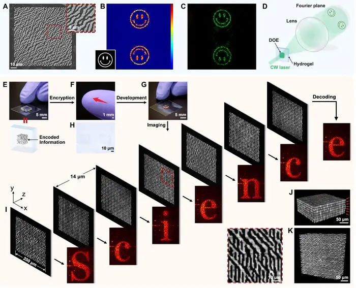
While conventional 3D nanoscale printers focus a laser point to serially process materials and take a long time to complete a design, Chen's invention changes the width of the laser's pulse to form patterned light sheets, allowing for a whole image containing hundreds of thousands of pixels (voxels) to be printed at once without compromising the axial resolution.
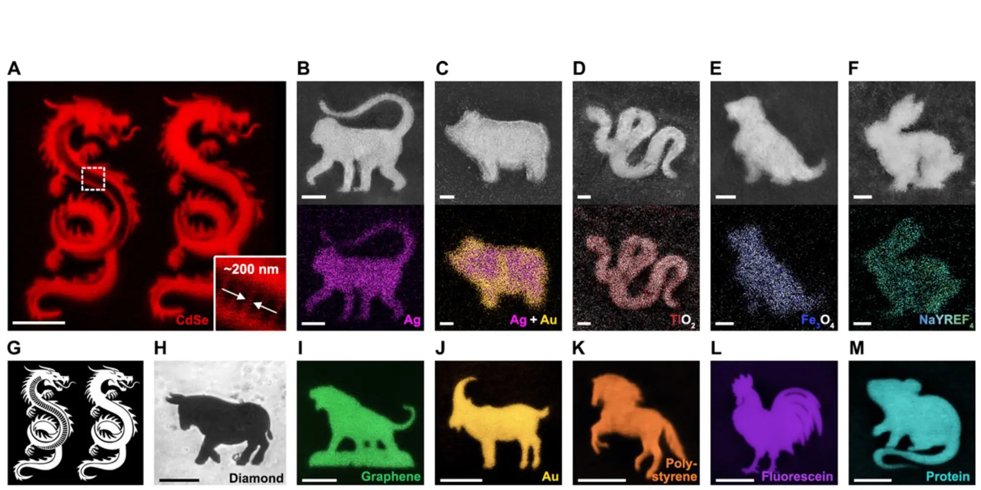
The manufacturing technique is called femtosecond project two-photon lithography, or FP-TPL. The method is up to 1,000 times faster than previous nanoprinting techniques and could lead to cost-effective large scale nanoprinting for use in in biotechnology, photonics or nanodevices.
For the process, researchers would direct the femtosecond two-photon laser to modify the network structure and pore size of the hydrogel, which then creates boundaries for water-dispersible materials. The hydrogel would then be immersed in water containing nanoparticles of metal, alloys, diamond, molecular crystals, polymers or fountain pen ink.
"Through fortuitous happenstance, the nanomaterials we tried were all attracted automatically to the printed pattern in hydrogel and assembled beautifully," Zhao said. "As the gel shrinks and dehydrates, the materials become even more densely packed and connect to each other."
For example, if a printed hydrogel is placed into a silver nanoparticle solution, the silver nanoparticles self-assemble to the gel along the laser-printed pattern. As the gel dries out, it can shrink to up to 13 times its original size, making the silver dense enough to form a nano silver wire and conduct electricity, Zhao said.
Because the gels are three-dimensional, printed patterns can be as well.
As a demonstration of the technique's use for encrypted optical storage — such as how CDs and DVDs are written and read with a laser — the team designed and built a seven-layer 3D nanostructure that read "SCIENCE" after it was optically decrypted.
How Small is Nano?
In the International System of Units, the prefix "nano" means one-billionth; so one nanometer is one-billionth of a meter. For example:
- There are 25,400,000 nanometers in one inch.
- A human hair is approximately 80,000- 100,000 nanometers wide.
- A single gold atom is about a third of a nanometer in diameter.
- On a comparative scale, if the diameter of a marble was one nanometer, then diameter of the Earth would be about one meter.
Each layer contained a 200x200-pixel hologram of a letter. After shrinking the sample the entire structure appears as a translucent rectangle under an optical microscope. One would need the right information on how much to expand the sample and where to shine a light through to read the information.
"Based on our result, the technique can pack 5 petabits worth of information in a tiny cubic centimeter of space. That's roughly 2.5 times of all U.S. academic research libraries combined." he said.
Zhao said that in the future the researchers' goal is to build functional nanodevices with multiple materials.
"In the end we would like to use the new technology to fabricate functional nanodevices, like nanocircuits, nanobiosensors, or even nanorobots for different applications," Zhao said. "We are only limited by our imagination."
In addition to Zhao and Chen, co-authors on the Science paper, "3D Nanofabrication via Ultrafast Laser Patterning and Kinetically-regulated Material Assembly," include Fei Han, Songyun Gu, Ni Zhao, all of the Chinese University of Hong Kong and Aleks Klimas, of Carnegie Mellon.
